一、Design Compiler综合
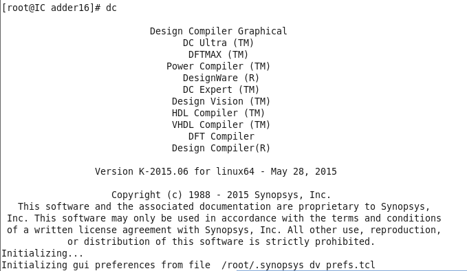
综合,在终端下输入dc
dv_use_pref_reader_version 1 {
# Design Vision version K-2015.06
# Preferences written on Sat Apr 1 19:39:54 2017
gui_set_var -name {read_pref_file} -value {true}
gui_create_pref_key -category {Globals} -key {allow_source_line_highlighting} -value_type {bool} -value {true}
gui_create_pref_key -category {Globals} -key {enable_cross_probe_from_rtl} -value_type {bool} -value {true}
gui_create_pref_key -category {Globals} -key {enable_rtl_source_view_in_congestion} -value_type {bool} -value {true}
gui_create_pref_key -category {Globals} -key {rtl_grouping_style} -value_type {string} -value {FileName-LineNumber Grouping}
gui_set_var -name {read_pref_file} -value {false}
}
一般.synopsys_dc.setup 文件有三个:①一个在synopsys的安装目录下,这个文件最好不要动;②一个在用户目录下,这个文件没事也不要动他;③还有一个当前工作目录下,也就是启动DC的目录下(没有就需要自己创建),这个是要我们自己写的,这个想怎么动就怎么动。我们配置DC的启动环境,就是在启动的目录创建.synopsys_dc.setup并且修改它。
这里,我们直接读入设计文件Adder16.v。
module Adder16 (ain, bin, cin, sout, cout, clk);
/* Sixteen Bit Adder Module */
output [15:0] sout;
output cout;
input [15:0] ain, bin;
input cin, clk;

wire [15:0] sout_tmp, ain, bin;
wire cout_tmp;
reg [15:0] sout, ain_tmp, bin_tmp;
reg cout, cin_tmp;

always @(posedge clk) begin
   cout = cout_tmp;
   sout = sout_tmp;
   ain_tmp = ain;
   bin_tmp = bin;
   cin_tmp = cin;
end
   assign {cout_tmp,sout_tmp} = ain_tmp + bin_tmp + cin_tmp;
endmodule
dc_shell> read_file Adder16.v
Information: Inferring file format verilog based on file name extension(s). (UID-1034)
Loading db file '/opt/Foundary_Library/TSMC90/aci/sc-x/synopsys/fast.db'
Loading db file '/opt/Foundary_Library/TSMC90/aci/sc-x/synopsys/fast_leakage.db'
Loading db file '/opt/Foundary_Library/TSMC90/aci/sc-x/synopsys/fastz.db'
Loading db file '/opt/Foundary_Library/TSMC90/aci/sc-x/synopsys/slow.db'
Loading db file '/opt/Foundary_Library/TSMC90/aci/sc-x/synopsys/typical.db'
Loading db file '/opt/Foundary_Library/TSMC90/aci/sc-x/synopsys/typical_leakage.db'
Loading db file '/opt/Synopsys/Synplify2015/libraries/syn/gtech.db'
Loading db file '/opt/Synopsys/Synplify2015/libraries/syn/standard.sldb'
Loading link library 'fast'
Loading link library 'fast_leakage'
Loading link library 'fastz'
Loading link library 'slow'
Loading link library 'typical'
Loading link library 'typical_leakage'
Loading link library 'gtech'
Loading verilog file '/home/IC/Documents/synplify/dw01/adder16/Adder16.v'
Detecting input file type automatically (-rtl or -netlist).
Reading with Presto HDL Compiler (equivalent to -rtl option).
Running PRESTO HDLC
Compiling source file /home/IC/Documents/synplify/dw01/adder16/Adder16.v
Inferred memory devices in process
in routine Adder16 line 13 in file
'/home/IC/Documents/synplify/dw01/adder16/Adder16.v'.
===============================================================================
| Register Name | Type | Width | Bus | MB | AR | AS | SR | SS | ST |
===============================================================================
| cout_reg | Flip-flop | 1 | N | N | N | N | N | N | N |
| sout_reg | Flip-flop | 16 | Y | N | N | N | N | N | N |
| ain_tmp_reg | Flip-flop | 16 | Y | N | N | N | N | N | N |
| bin_tmp_reg | Flip-flop | 16 | Y | N | N | N | N | N | N |
| cin_tmp_reg | Flip-flop | 1 | N | N | N | N | N | N | N |
===============================================================================
Presto compilation completed successfully.
Current design is now '/home/IC/Documents/synplify/dw01/adder16/Adder16.db:Adder16'
Loaded 1 design.
Current design is 'Adder16'.
Adder16
如果我们使用tcl文件,直接运行命令:
source adder16.tcl
set design "adder16"
current_design Adder16
# Define design environment
set_load 2.2 sout
set_load 1.5 cout


# Define design constraints
set_input_delay 1.35 -clock $clk_name {ain bin}
set_input_delay 3.5 -clock $clk_name cin
set_max_area 0

compile
write_file -format ddc -hierarchy -output adder16.ddc
write -f verilog -hierarchy -output adder16.v
write_sdc adder16.sdc
运行结果:
dc_shell> source adder16.tcl
Current design is 'Adder16'.

Information: There are 6 potential problems in your design. Please run 'check_design' for more information. (LINT-99)


Warning: Operating condition fast set on design Adder16 has different process,
voltage and temperatures parameters than the parameters at which target library
fast_leakage is characterized. Delays may be inaccurate as a result. (OPT-998)

  Beginning Pass 1 Mapping
  ------------------------
  Processing 'Adder16_DW01_add_0'
  Processing 'Adder16'

  Updating timing information
Information: Updating design information... (UID-85)

  Beginning Implementation Selection
  ----------------------------------

  Beginning Mapping Optimizations  (Medium effort)
  -------------------------------

                                  TOTAL
   ELAPSED            WORST NEG   SETUP    DESIGN
    TIME      AREA      SLACK     COST    RULE COST         ENDPOINT
  --------- --------- --------- --------- --------- -------------------------
    0:00:01    1875.5      0.00       0.0      55.7
    0:00:01    1875.5      0.00       0.0      55.7
    0:00:01    1875.5      0.00       0.0      55.7
    0:00:01    1875.5      0.00       0.0      55.7
    0:00:01    1875.5      0.00       0.0      55.7
    0:00:01    1120.5      0.00       0.0      55.7
    0:00:01    1120.5      0.00       0.0      55.7
    0:00:01    1120.5      0.00       0.0      55.7
    0:00:01    1120.5      0.00       0.0      55.7
    0:00:01    1120.5      0.00       0.0      55.7
    0:00:01    1289.8      0.00       0.0       2.2
    0:00:02    1298.3      0.00       0.0       0.2
    0:00:02    1298.3      0.00       0.0       0.2
    0:00:02    1298.3      0.00       0.0       0.2
    0:00:02    1298.3      0.00       0.0       0.2


  Beginning Delay Optimization Phase
  ----------------------------------

                                  TOTAL
   ELAPSED            WORST NEG   SETUP    DESIGN
    TIME      AREA      SLACK     COST    RULE COST         ENDPOINT
  --------- --------- --------- --------- --------- -------------------------
    0:00:02    1298.3      0.00       0.0       0.2
    0:00:02    1298.3      0.00       0.0       0.2
    0:00:02    1298.3      0.00       0.0       0.2


  Beginning Design Rule Fixing  (max_capacitance)
  ----------------------------

                                  TOTAL
   ELAPSED            WORST NEG   SETUP    DESIGN
    TIME      AREA      SLACK     COST    RULE COST         ENDPOINT
  --------- --------- --------- --------- --------- -------------------------
    0:00:02    1298.3      0.00       0.0       0.2


  Beginning Area-Recovery Phase  (max_area 0)
  -----------------------------

                                  TOTAL
   ELAPSED            WORST NEG   SETUP    DESIGN
    TIME      AREA      SLACK     COST    RULE COST         ENDPOINT
  --------- --------- --------- --------- --------- -------------------------
    0:00:02    1298.3      0.00       0.0       0.2
    0:00:02    1298.3      0.00       0.0       0.2
    0:00:02    1298.3      0.00       0.0       0.2
    0:00:02    1298.3      0.00       0.0       0.2
    0:00:02    1298.3      0.00       0.0       0.2
    0:00:02    1298.3      0.00       0.0       0.2
    0:00:02    1286.3      0.00       0.0       0.2
    0:00:02    1286.3      0.00       0.0       0.2
    0:00:02    1286.3      0.00       0.0       0.2
    0:00:02    1286.3      0.00       0.0       0.2
    0:00:02    1286.3      0.00       0.0       0.2
    0:00:02    1286.3      0.00       0.0       0.2
    0:00:02    1286.3      0.00       0.0       0.2
    0:00:02    1286.3      0.00       0.0       0.2
    0:00:02    1286.3      0.00       0.0       0.2
    0:00:02    1286.3      0.00       0.0       0.2
    0:00:02    1286.3      0.00       0.0       0.2
    0:00:02    1286.3      0.00       0.0       0.2
Loading db file '/opt/Foundary_Library/TSMC90/aci/sc-x/synopsys/fast.db'
Loading db file '/opt/Foundary_Library/TSMC90/aci/sc-x/synopsys/fastz.db'
Loading db file '/opt/Foundary_Library/TSMC90/aci/sc-x/synopsys/slow.db'
Loading db file '/opt/Foundary_Library/TSMC90/aci/sc-x/synopsys/typical.db'


Note: Symbol # after min delay cost means estimated hold TNS across all active scenarios


  Optimization Complete
  ---------------------
Writing ddc file 'adder16.ddc'.
输出的文件

二、ICC布局布线
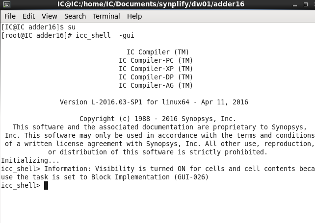
在终端启动icc_shell -gui
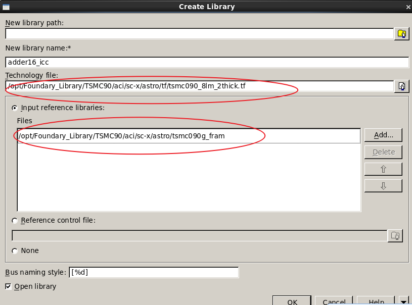
接着点击File->Create Library
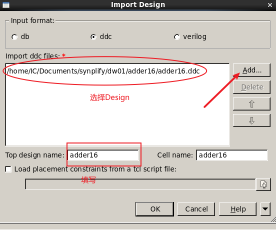
创建完Library之后导入Design
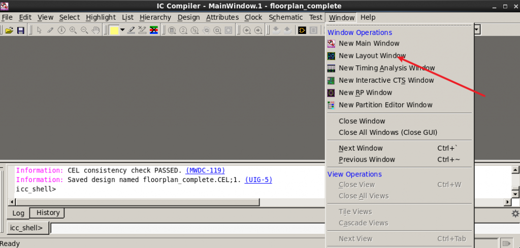
读入设计后,进入Layout窗口
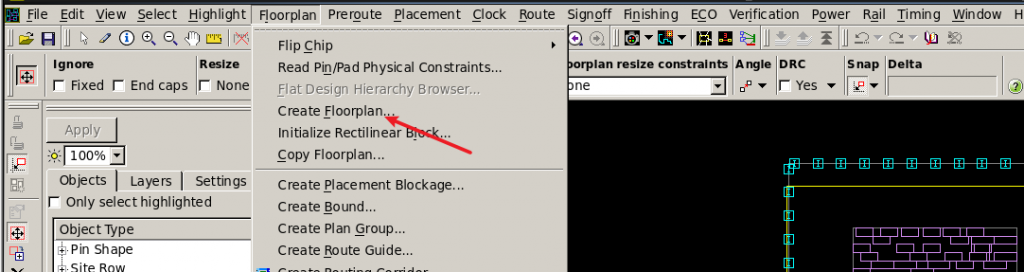
进入Layout Window后创建Floorplan。
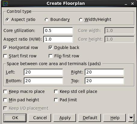
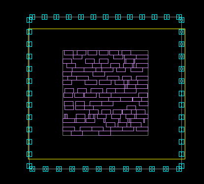
创建完Floorplan之后,进入ICC主窗口create_fp_placement
随时保存一下,File->Save Design。
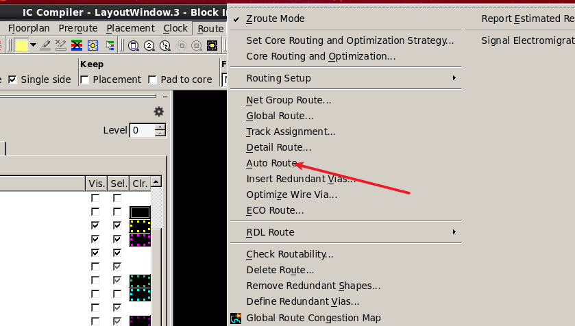
接着,进行自动布线:
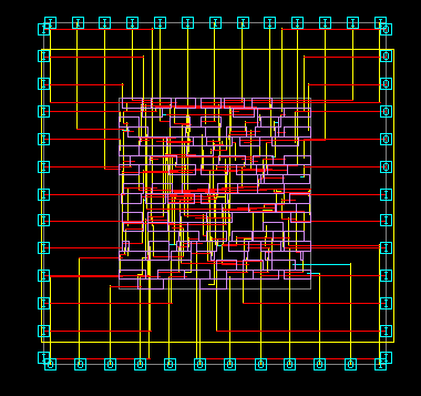
自动布线之后的结果
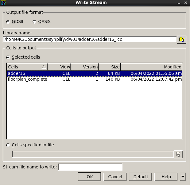
写入GDSII文件File->Export->Write Stream
将gds文件导入L-edit中查看
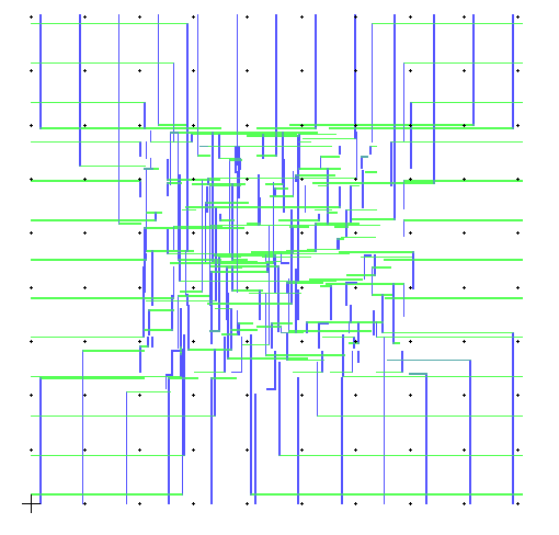
发现连线导出了,但是用到的cell没有出来
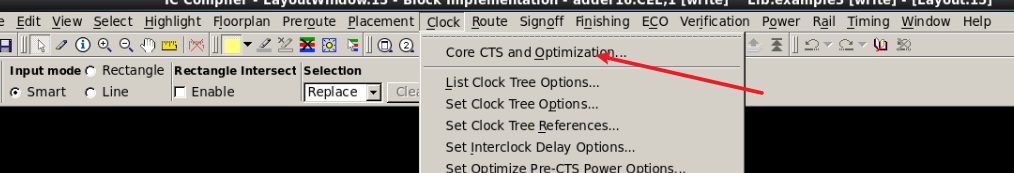
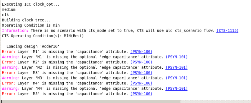
时钟树综合(CTS),命令是clock_opt。也可以在图形界面选择Clock->Core CTS and Optimization。
这里需要注意一点,如果你的tf文件中没有capacitance这一项,就会报错:
我们在tf文件中加上下面红字的三行,重新建立Library,导入Design,进行floorplan和CTS。
Layer		"M1" {
		layerNumber			= 31
		maskName			= "metal1"
		isDefaultLayer			= 1
		visible				= 1
		selectable			= 1
		blink				= 0
		color				= "cyan"
		lineStyle			= "solid"
		pattern				= "dot"
		pitch				= 0.28
		defaultWidth			= 0.12
		minWidth			= 0.12
		minSpacing			= 0.12
		maxWidth			= 12
		maxCurrDensity			= 20
		unitMinCapacitance		= 3.89e-05
		unitNomCapacitance		= 4.22e-05
		unitMaxCapacitance		= 4.61e-05
		unitMinResistance		= 0.00013
		unitNomResistance		= 0.00013
		unitMaxResistance		= 0.00013
		fatTblDimension			= 4
		fatTblThreshold			= (0,0.305,1.505,4.505)
		fatTblParallelLength		= (0,0.525,1.505,4.505)
		fatTblSpacing			= (0.12,0.17,0.5,1.5,
						   0.17,0.17,0.5,1.5,
						   0.5,0.5,0.5,1.5,
						   1.5,1.5,1.5,1.5)
		minArea				= 0.058
		minEnclosedArea			= 0.2
}
就会看到CTS Successful:
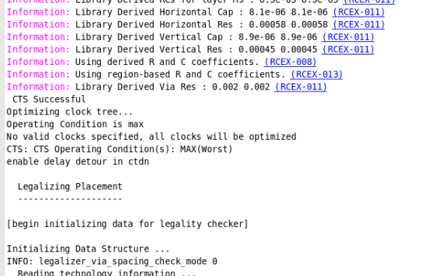
这里列出所有控制台输出:
icc_shell> clock_opt
Warning: Starting from the 2011.09-SP4 release, clock_opt will NOT perform congestion-driven placement by default. (PSYN-1111)

The options for clock_opt:
--------------------------
COPT:  Clock Tree Synthesis                 : Yes
COPT:  Post CTS Optimization                : Yes
COPT:  Concurrent Clock/Data Optimization   : No
COPT:  Operation Condition                  : max
COPT:  Balance Inter Clock Delay            : No
COPT:  Route Clock Nets                     : Yes
COPT:  Update Clock Latency                 : No
COPT:  Optimize Hold for All Clocks         : No
COPT:  Optimize Hold Timing Only            : No
COPT:  Optimize DFT                         : No
COPT:  Area Recovery                        : No
COPT:  Size Only                            : No
COPT:  In Place Size Only                   : No
COPT:  Congestion removal                   : No
COPT:  Optimize Power                       : No
---------------------------------------------------

Executing ICC clock_opt...
medium
*
Building clock tree...
Operating Condition is max
Information: There is no scenario with cts_mode set to true, CTS will use old cts_scenario flow. (CTS-1115)
CTS: CTS Operating Condition(s): MAX(Worst)

  Loading design 'Adder16'
Warning: Layer 'M1' is missing the optional 'edge capacitance' attribute. (PSYN-101)
Warning: Layer 'M2' is missing the optional 'edge capacitance' attribute. (PSYN-101)
Warning: Layer 'M3' is missing the optional 'edge capacitance' attribute. (PSYN-101)
Warning: Layer 'M4' is missing the optional 'edge capacitance' attribute. (PSYN-101)
Warning: Layer 'M5' is missing the optional 'edge capacitance' attribute. (PSYN-101)
Warning: Layer 'M6' is missing the optional 'edge capacitance' attribute. (PSYN-101)
Warning: Layer 'M7' is missing the optional 'edge capacitance' attribute. (PSYN-101)
Warning: Layer 'M8' is missing the optional 'edge capacitance' attribute. (PSYN-101)
Warning: Layer 'M9' is missing the optional 'edge capacitance' attribute. (PSYN-101)


Information: Library Manufacturing Grid(GridResolution) : 5
Information: Time Unit from Milkyway design library: 'ns'
Information: Design Library and main library timing units are matched - 1.000 ns.
Information: Resistance Unit from Milkyway design library: 'kohm'
Information: Design Library and main library resistance units are matched - 1.000 kohm.
Information: Capacitance Unit from Milkyway design library: 'pf'
Information: Design Library and main library capacitance units are matched - 1.000 pf.
[begin initializing data for legality checker]

Initializing Data Structure ...
INFO: legalizer_via_spacing_check_mode 0
  Reading technology information ...
    Technology table contains 9 routable metal layers
    This is considered as a 9-metal-layer design
    Reading library information from DB ...
  Reading misc information ...
    array <unit> has 0 vertical and 17 horizontal rows
    GRC ref loc X corrected
    GRC ref loc Y corrected
  Checking information read in ...
    design style = Horizontal masters, Horizontal rows

  Preprocessing design ...
    splitting rows by natural obstacles ...
... design style 0
... number of base array 1 0
INFO:... use original rows...
[end initializing data for legality checker]
Setting the GR Options
Information: The distance unit in Capacitance and Resistance is 1 micron. (RCEX-007)
Information: The RC model used is library 1D. (RCEX-015)
Information: Library Derived Cap for layer M1 : 5.1e-06 5.1e-06 (RCEX-011)
Information: Library Derived Res for layer M1 : 0.0011 0.0011 (RCEX-011)
Information: Library Derived Cap for layer M2 : 5.9e-06 5.9e-06 (RCEX-011)
Information: Library Derived Res for layer M2 : 0.00058 0.00058 (RCEX-011)
Information: Library Derived Cap for layer M3 : 5.9e-06 5.9e-06 (RCEX-011)
Information: Library Derived Res for layer M3 : 0.00058 0.00058 (RCEX-011)
Information: Library Derived Cap for layer M4 : 5.9e-06 5.9e-06 (RCEX-011)
Information: Library Derived Res for layer M4 : 0.00058 0.00058 (RCEX-011)
Information: Library Derived Cap for layer M5 : 5.9e-06 5.9e-06 (RCEX-011)
Information: Library Derived Res for layer M5 : 0.00058 0.00058 (RCEX-011)
Information: Library Derived Cap for layer M6 : 5.9e-06 5.9e-06 (RCEX-011)
Information: Library Derived Res for layer M6 : 0.00058 0.00058 (RCEX-011)
Information: Library Derived Cap for layer M7 : 5.9e-06 5.9e-06 (RCEX-011)
Information: Library Derived Res for layer M7 : 0.00058 0.00058 (RCEX-011)
Information: Library Derived Cap for layer M8 : 1.8e-05 1.8e-05 (RCEX-011)
Information: Library Derived Res for layer M8 : 6.5e-05 6.5e-05 (RCEX-011)
Information: Library Derived Cap for layer M9 : 1.8e-05 1.8e-05 (RCEX-011)
Information: Library Derived Res for layer M9 : 6.5e-05 6.5e-05 (RCEX-011)
Information: Library Derived Horizontal Cap : 8.1e-06 8.1e-06 (RCEX-011)
Information: Library Derived Horizontal Res : 0.00058 0.00058 (RCEX-011)
Information: Library Derived Vertical Cap : 8.9e-06 8.9e-06 (RCEX-011)
Information: Library Derived Vertical Res : 0.00045 0.00045 (RCEX-011)
Information: Using derived R and C coefficients. (RCEX-008)
Information: Using region-based R and C coefficients. (RCEX-013)
Information: Library Derived Via Res : 0.002 0.002 (RCEX-011)
LR: Layer M3: Average tracks per gcell 9.0, utilization 0.00
LR: Layer M4: Average tracks per gcell 9.0, utilization 0.00
LR: Layer M5: Average tracks per gcell 9.0, utilization 0.00
LR: Layer M6: Average tracks per gcell 9.0, utilization 0.00
LR: Layer M7: Average tracks per gcell 9.0, utilization 0.00
LR: Layer M8: Average tracks per gcell 2.9, utilization 0.00
LR: Layer M9: Average tracks per gcell 2.9, utilization 0.00
LR: Clock routing service standing by
Using cts integrated global router
CTS: Blockage Aware Algorithm
CTS: Top-Level OCV Path Sharing not effective when timing derating is too low
[begin initializing data for legality checker]

Initializing Data Structure ...
INFO: legalizer_via_spacing_check_mode 0
  Reading technology information ...
    Technology table contains 9 routable metal layers
    This is considered as a 9-metal-layer design
    Reading library information from DB ...
  Reading misc information ...
    array <unit> has 0 vertical and 17 horizontal rows
    GRC ref loc X corrected
    GRC ref loc Y corrected
  Checking information read in ...
    design style = Horizontal masters, Horizontal rows

  Preprocessing design ...
    splitting rows by natural obstacles ...
... design style 0
... number of base array 1 0
INFO:... use original rows...
[end initializing data for legality checker]
CTS: Region Aware Algorithm is automatically turned off when design has no region or only has one region.
CTS-Warning: clock root not found
CTS: ==================================================
CTS: Start DRC fixing beyond exceptions
CTS: Blockage Aware Algorithm
CTS: Top-Level OCV Path Sharing not effective when timing derating is too low
[begin initializing data for legality checker]

Initializing Data Structure ...
INFO: legalizer_via_spacing_check_mode 0
  Reading technology information ...
    Technology table contains 9 routable metal layers
    This is considered as a 9-metal-layer design
    Reading library information from DB ...
  Reading misc information ...
    array <unit> has 0 vertical and 17 horizontal rows
    GRC ref loc X corrected
    GRC ref loc Y corrected
  Checking information read in ...
    design style = Horizontal masters, Horizontal rows

  Preprocessing design ...
    splitting rows by natural obstacles ...
... design style 0
... number of base array 1 0
INFO:... use original rows...
[end initializing data for legality checker]
CTS: Region Aware Algorithm is automatically turned off when design has no region or only has one region.
CTS-Warning: clock root not found
CTS: DRC fixing initialization error. Abort
CTS: ==================================================
Information: The distance unit in Capacitance and Resistance is 1 micron. (RCEX-007)
Information: The RC model used is library 1D. (RCEX-015)
Information: Library Derived Cap for layer M1 : 5.1e-06 5.1e-06 (RCEX-011)
Information: Library Derived Res for layer M1 : 0.0011 0.0011 (RCEX-011)
Information: Library Derived Cap for layer M2 : 5.9e-06 5.9e-06 (RCEX-011)
Information: Library Derived Res for layer M2 : 0.00058 0.00058 (RCEX-011)
Information: Library Derived Cap for layer M3 : 5.9e-06 5.9e-06 (RCEX-011)
Information: Library Derived Res for layer M3 : 0.00058 0.00058 (RCEX-011)
Information: Library Derived Cap for layer M4 : 5.9e-06 5.9e-06 (RCEX-011)
Information: Library Derived Res for layer M4 : 0.00058 0.00058 (RCEX-011)
Information: Library Derived Cap for layer M5 : 5.9e-06 5.9e-06 (RCEX-011)
Information: Library Derived Res for layer M5 : 0.00058 0.00058 (RCEX-011)
Information: Library Derived Cap for layer M6 : 5.9e-06 5.9e-06 (RCEX-011)
Information: Library Derived Res for layer M6 : 0.00058 0.00058 (RCEX-011)
Information: Library Derived Cap for layer M7 : 5.9e-06 5.9e-06 (RCEX-011)
Information: Library Derived Res for layer M7 : 0.00058 0.00058 (RCEX-011)
Information: Library Derived Cap for layer M8 : 1.8e-05 1.8e-05 (RCEX-011)
Information: Library Derived Res for layer M8 : 6.5e-05 6.5e-05 (RCEX-011)
Information: Library Derived Cap for layer M9 : 1.8e-05 1.8e-05 (RCEX-011)
Information: Library Derived Res for layer M9 : 6.5e-05 6.5e-05 (RCEX-011)
Information: Library Derived Horizontal Cap : 8.1e-06 8.1e-06 (RCEX-011)
Information: Library Derived Horizontal Res : 0.00058 0.00058 (RCEX-011)
Information: Library Derived Vertical Cap : 8.9e-06 8.9e-06 (RCEX-011)
Information: Library Derived Vertical Res : 0.00045 0.00045 (RCEX-011)
Information: Using derived R and C coefficients. (RCEX-008)
Information: Using region-based R and C coefficients. (RCEX-013)
Information: Library Derived Via Res : 0.002 0.002 (RCEX-011)
 CTS Successful
Optimizing clock tree...
Operating Condition is max
No valid clocks specified, all clocks will be optimized
CTS: CTS Operating Condition(s): MAX(Worst)
enable delay detour in ctdn

  Legalizing Placement
  --------------------

[begin initializing data for legality checker]

Initializing Data Structure ...
INFO: legalizer_via_spacing_check_mode 0
  Reading technology information ...
    Technology table contains 9 routable metal layers
    This is considered as a 9-metal-layer design
    Reading library information from DB ...
  Reading misc information ...
    array <unit> has 0 vertical and 17 horizontal rows
    GRC ref loc X corrected
    GRC ref loc Y corrected
  Checking information read in ...
    design style = Horizontal masters, Horizontal rows

  Preprocessing design ...
    splitting rows by natural obstacles ...
... design style 0
... number of base array 1 0
INFO:... use original rows...
[end initializing data for legality checker]

****************************************
  Report : Chip Summary
  Design : Adder16
  Version: L-2016.03-SP1
  Date   : Sun Jun  5 01:58:50 2022
****************************************
Std cell utilization: 70.09%  (1823/(2601-0))
(Non-fixed + Fixed)
Std cell utilization: 70.09%  (1823/(2601-0))
(Non-fixed only)
Chip area:            2601     sites, bbox (0.00 0.00 42.84 42.84) um
Std cell area:        1823     sites, (non-fixed:1823   fixed:0)
                      100      cells, (non-fixed:100    fixed:0)
Macro cell area:      0        sites
                      0        cells
Placement blockages:  0        sites, (excluding fixed std cells)
                      0        sites, (include fixed std cells & chimney area)
                      0        sites, (complete p/g net blockages)
Routing blockages:    0        sites, (partial p/g net blockages)
                      0        sites, (routing blockages and signal pre-route)
Lib cell count:       5
Avg. std cell width:  5.26 um
Site array:           unit     (width: 0.28 um, height: 2.52 um, rows: 17)
Physical DB scale:    1000 db_unit = 1 um


****************************************
  Report : pnet options
  Design : Adder16
  Version: L-2016.03-SP1
  Date   : Sun Jun  5 01:58:50 2022
****************************************


--------------------------------------------------------------------
Layer      Blockage   Min_width   Min_height   Via_additive     Density
--------------------------------------------------------------------
M1         none          ---         ---       via additive      ---
M2         none          ---         ---       via additive      ---
M3         none          ---         ---       via additive      ---
M4         none          ---         ---       via additive      ---
M5         none          ---         ---       via additive      ---
M6         none          ---         ---       via additive      ---
M7         none          ---         ---       via additive      ---
M8         none          ---         ---       via additive      ---
M9         none          ---         ---       via additive      ---

****************************************
  Report : Legalize Displacement
  Design : Adder16
  Version: L-2016.03-SP1
  Date   : Sun Jun  5 01:58:50 2022
****************************************

No cell displacement.


  Placement Legalization Complete
  -------------------------------

Information: Updating database...
Unsetting the GR Options
LR: 0 out of 0 clock nets rerouted
LR: Clock routing service terminated
Invalidate design extracted status
Optimize clock tree UnSuccessful... Aborting clock_opt
0
时钟树综合之后,可以使用report_timing命令来看报告:
三、Milkyway的使用
为何要用 Milkyway 和 NDM?Milkyway 是供 ICC 使用,NDM 则是供 ICC2 使用。这里简单说下,MIlkyway 是对应 GDS 的抽象化,因为它文件不大,信息量够 PR 工具使用。有人可能会说直接用 GDS,试问你是想玩死工具吗?Milkyway 的制作其实就包含了三类信息,Blockage,Pin,Via,就是通常所说的 BPV。简而言之,就是 Milkyway 就是告诉 tool,这个 ip 有多大,有哪些 signal pin,power ground pin, 哪些地方有 blockage,在哪些地方可以打孔。【引用自这里】
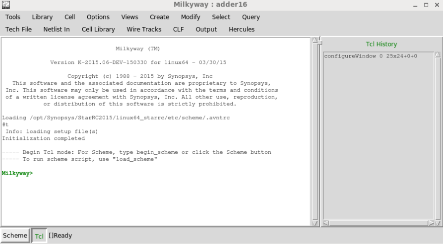
Milkway图形界面启动
Milkyway -galaxy -tcl
物理库:描述了工艺层次,工艺规则以及标准单元等IP的形状大小,端口位置信息,目前业内标准是(.lef)格式,但是Synopsys的ICC使用Milkway格式的数据库,其中的fram view就是物理库,其本质和lef一样,ICC2放弃了Milkyway,使用(.db)和(.lef)生成的ndm作为参考库创建ndb。通常情况下,IO单元和标准单元的Milkyway库由IP提供商提供,而宏单元(Macro)的Milkway需要后端设计人员用Synopsys专门的EDA工具Milkyway根据宏单元的GDS文件或lef文件生成。
对于每一个工艺的参考库,都有专门的技术文件(Technology File)来说明其工艺的参数信息,技术文件简称(.tf)文件,产生Milkyway物理库和ndb时需要用到此文件。
技术文件通常由工艺厂提供,文件主要包含了每层掩膜层的层号,连接层信息,子啊EDA工具中显示的颜色与线条,最小宽度,最小面积等信息。ICC就是根基技术文件中的描述的金属层和通孔层的设计规则进行布局布线的。
四、Liberty文件详解
4.0 时序分析基本概念介绍——时序库Lib
今天主要介绍的时序概念是时序库lib犀利士 rong>,全称liberty library format(以• lib结尾),
用于描述物理单元的时序和功耗信息的重要库文件。lib库是最基本的时序库,通常文件很大,分为两个部分,
第一部分定义了物理单元库的基本属性,它包括:
1)单元库名称,文件版本,产生日期及单元的PVT环境等。
2)定义电压,电流,电容,时间等基本单位。
3 ) 定义电路传输时间和信号转换时间的电压百分比。
我们来看一个基本的lib时序库:
library(xxx18) { #库名称
delay_model : table_lookup; #采用查表延时模型计算延时
revision : 1.0; #库的版本
date : “Sat Mar 2 15:37:50 2012”; #库的创建时间
time_unit : “1ns”; #定义时间基本单位
voltage_unit : “1V”; #定义电压基本单位
current_unit : “1uA”; #定义电流基本单位
pulling_resistance_unit : “1kohm”; #定义电阻基本单位
leakage_power_unit : “1pW”; #定义功耗基本单位
capacitive_load_unit (1.0,pf); #定义负载基本单位
nom_process : 1; #定义时序库工艺
nom_temperature : -40; #定义时序库温度
nom_voltage : 0.72; #定义时序库电压
operating_conditions(fast) { #定义互连线模型
process : 1;
temperature : -40;
voltage : 0.72;
tree_type : balanced_tree
}
/* threshold definitions */
slew_lower_threshold_pct_fall : 10.0; #定义信号转换模型
slew_upper_threshold_pct_fall : 90.0;
slew_lower_threshold_pct_rise : 10.0;
slew_upper_threshold_pct_rise : 90.0;
input_threshold_pct_fall : 50.0; #定义延迟模型
input_threshold_pct_rise : 50.0;
output_threshold_pct_fall : 50.0;
output_threshold_pct_rise : 50.0;
第二部分是每个单元的具体信息,包括单元的延迟时间,泄漏功耗,内部功耗等。它们以lookup table的形式来表示,这里一个非常重要的概念就是lookup table,它是一种三维数据查找表,整个lib文件都是通过该种查找方式来得到所需要的信息。例如延迟时间作为输出信号负载(output load)和输入信号转换时间(input transition)的函数列表。
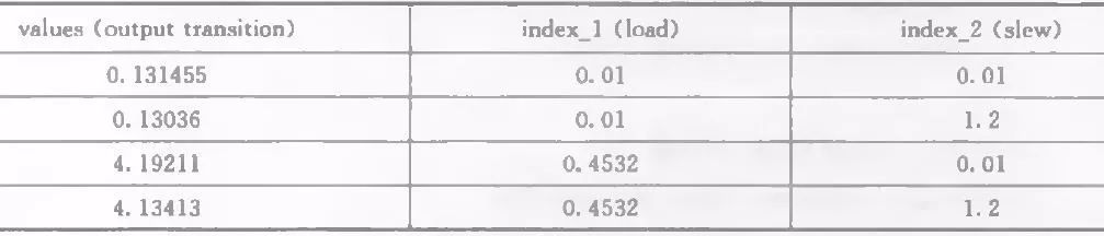
我们来看一个look up table的查找方式:
lu_table_template(delay_template_2x2){
variable_1:total_output_net_capacitance;
variable_2:input_net_transition;
index 1(“1000.0,1001.0”);
index _2( ” 1000.0, 1001.0″ ) ;
}
rise_transition (delay_template_2x2) {
index_l( “0.01,0.4532” ) ;
index_2( “0.01,1.2” );
values (“0 .131455 , 0.131036 ” ,
“4.19211,4.13413”) ;
}
上诉语句定义了一个名字叫为delay_template_2x2的lookup table,可以理解为一个模板,有两个变量variable_1和variable_2组成。variable_1代表total_output_net_capacitance,variable_2代表input_net_transition。每个变量是两个断点组成。lookup table的名字是任意的,而变量可以是一个,两个或三个,每个断点的数量一般没有限制。
lookup table的第二部分则描述了具体哪个功能调用了上述模板,rise_transition描述的是单元输出信号的上升时间。它调用的就是由lu_table_template 定义的名为delay_template_2x2的模板。rise_transiton 中 index_1和 index_2是与上升时间相关的两个变量,如果想知道它们分别代表哪个一个变量就需要到delay_template_2x2的模板中查找,这里我们知道index_1代表输出pin的连线负载电容,index_2代表输入信号transition。
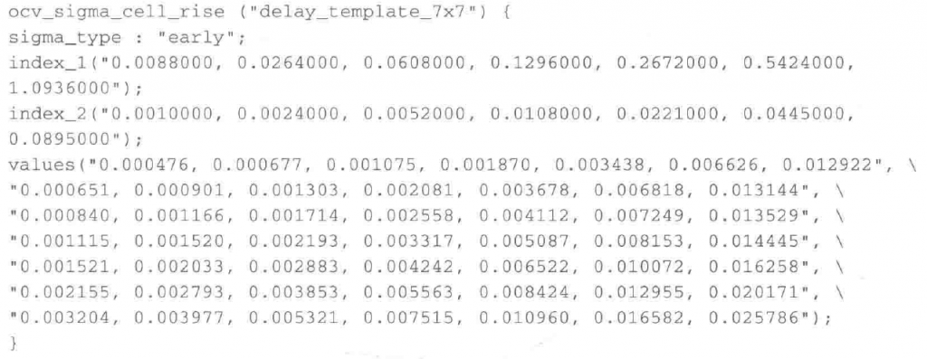
values与index可以表达为value=f(index_1,index_2)。当输出端线负载为0. 01,输入斜率为0. 01时,输出上升时间为0.131455。当输出线负载为0.01,输人斜率为1 .2时,输出上升时间为0.13036。同理,当输出端线负载为0.4532,输入斜率分别为0.01和1.2 时,对应另外两个上升时间。如下图所示:
接着在cell描述部分,我们会看到以下内容:
cell (BUFX1) {
cell_footprint : buf; #定义引脚名称,进行优化时具有相同引脚名称的单元才可以交换
area : 13.305600; #定义单元面积大小
pin(A) {
direction : input; #定义端口A为输入端口
capacitance : 0.002357; #定义端口A的电容
}
pin(Y) {
direction : output; #定义端口Y为输出端口
capacitance : 0.0; #定义端口Y的电容
function : “A”; #定义端口Y是同A的操作
internal_power() { #定义单元内部功耗
related_pin : “A”; #定义相关输入信号
rise_power(energy_template_5x5) { #定义端口Y上升所消耗的功耗
index_1 (“0.025, 0.08, 0.3, 0.7, 1.2”);
index_2 (“0.00035, 0.021, 0.0385, 0.084, 0.147”);
values (
“0.013041, 0.010646, 0.010132, 0.008511, 0.006121”,
“0.015728, 0.012869, 0.012227, 0.010567, 0.008178”,
“0.023086, 0.020760, 0.019879, 0.017596, 0.014946”,文件太长,只截取部分,rise_power的 index_1和index_2的内容可以在文件前面的lookup table模板中查找得到,该cell的剩余其他时序和功耗参数也是类似描述,不一一解释了。
4.1 faults_lut_template
library ( my_library_name ) {
…
faults_lut_template ( my_faults_temp ) {
variable_1 : fab_name;
variable_2 : time_range;
index_1 ( " fab1, fab2, fab3 ");
index_2 (" 2005.01, 2005.07, 2006.01, 2006.07 ");
}
…
cell ( and2 ) {
…
functional_yield_metric () {
average_number_of_faults ( my_faults_temp ) {
values ( " 73.5, 78.8, 85.0, 92 ",
" 74.3, 78.7, 84.8, 92.2 ",
" 72.2, 78.1, 84.3, 91.0 " );
}
}
…
} /* end of cell */
} /* end of library */
This example specifies fault data for three fabs (fab1, fab2, and fab3).
For fab1:
● 73.5 is the average number of faults due to functional yield loss mechanisms
(that is, random defects) for the time range 2005.01 to 2005.06
● 78.8 is the average number of faults due to functional yield loss mechanisms for
the time range 2005.07 to 2005.12
● 85.0 is the average number of faults due to functional yield loss mechanisms for
the time range 2006.01 to 2006.07
● 92.0 is the average number of faults due to functional yield loss mechanisms for
the time range 2006.07 or later
For fab2:
● 74.3 is the average number of faults due to functional yield loss mechanisms for
the time range 2005.01 to 2005.06
● 78.7 is the average number of faults due to functional yield loss mechanisms for
the time range 2005.07 to 2005.12
● 84.8 is the average number of faults due to functional yield loss mechanisms for
the time range 2006.01 to 2006.07
● 92.2 is the average number of faults due to functional yield loss mechanisms for
the time range 2006.07 or later
And so on for fab3.
4.2 浅谈K库
首先要解释什么是K库,记得当年查遍K开头的单词也没有找到答案,后来才知道所谓的K指的是谐音“characterization”,意思是表征。
所谓的K库指的是将标准单元stdcell的特性用lib的形式表征出来,具体是将stdcell的gds抽取出带rc信息的我spice网表,通常指的是lpe_spice网表,加上spice model用给定的K库 flow生成对应不同PVT下的lib,K库flow的本质就是spice仿真,并将仿真得到的结果加一定的margin如delay/slew/constraint等等,margin加多大还是取决于foundary,foundary会通过大量的silicon结果进行correlation得到的,因此flow基本还是要从foundary那里获取。
最后解释一下为什么要K库,使用库来signff是目前主流的signoff方式,相比于spice仿真来说,最大的优点就是快,使用相应的signoff工具对lib信息进行抽取和计算即可,但同时也给到silicon的correlation验证增加了一个环节即lib to spice,spice to silicon,但是也没有办法,随着工艺的演进,一个设计中晶体管数量已经达到百亿千亿级别,无论是从时间还是资源上仿真已经远远无法满足,而且即使是lib signoff,目前稍复杂的设计对signoff corner的要求已经能达到几百个,但目前没有更好的更简单有效的signoff方式,只能是依赖工具和服务器在算力和算法上的提升。
当然库的内容也是在不断发生演进,从nldm到ccs到lvf,库的内容一直在不断丰满,同时也会使signoff变得更加精准。
————————————————
版权声明:本文为CSDN博主「林聊ic」的原创文章,遵循CC 4.0 BY-SA版权协议,转载请附上原文出处链接及本声明。
原文链接:https://blog.csdn.net/weixin_51064938/article/details/121111468
参考公众号:公众号-K库自习室LibChar现已更名为【单元库特征化及建库技术】,ID:libchar(ID不变),欢迎关注!
K库工具liberate手册 liberate.pdf【重要】
K库,根据eetop上的帖子运行如下:
Standard-cell characterization
4.3 时序弧
《集成电路静态时序分析与建模》
静态时序分析是基于时序弧(timing arc)数据的时序分析。时序弧是用来描述两个节点延时信息的数据,时序弧的信息一般分为连线延时和单元延时。连线延时是单元输出端口和扇出网络负载的延时信息;单元延时是单元输入端口到输出端口的延时信息。因此一条完整路径的时序信息计算由连线延时和单元延时组成。
4.4 片上随机变化系数(POCV)
参数化芯片变化相关分析模式
随着制造工艺越来越先进,比如14nm工艺下,AOCV分析模式中动态设置时序减免值得方法已经不能满足当前时序分析精度的要求,其时序分析结果的悲观性也无法很好地改变。
AOCV分析模式需要先分析时序路径的逻辑深度和物理距离两个因素,再设置时序减免值,导致其时序分析工作量增大。因此对于比较大的设计,整个设计的时序分析计算时间会增加。
同样是因为AOCV分析模式需要基于分析时序路径的逻辑深度和物理距离因素来设置时序减免值,如果设计中途改动了时序路径和逻辑深度,比如时序优化中增加了缓冲器或者移除了缓冲器,那么其时序路径的逻辑深度改变后就需要重新设置时序减免值,这样会导致时序分析时需要不停地刷新减免值设置,并重新计算。
《集成电路静态时序分析与建模》 p102
在时序信息文件中通过POCV电平转换或负载查找表直接定义。
POCV分析模式的数据输入格式有两种,一种是使用与AOCV一样的查找表数据输入格式,POCV分析模式查找表格式如下:
version:4.0
ocvm_type:pocvm
object_type:lib_cell
rf_type:rise_fall
delay_type:cell
derate_type:early
object_spec:lib28nm/invx*
coefficient:0.05
POCV电平转换或父子啊查找表的格式(liberty variation format)简称LVF,如下图所示。
4.5 多周期路径、伪路径
《集成电路静态时序分析与建模》 p122
4.6 时序弧——Multiple mode Descriptions
Liberty User Manual 7-30
library (MODE_EXAMPLE) {
    delay_model : "table_lookup";
    time_unit : "1ns";
    voltage_unit : "1V";
    current_unit : "1mA";
    pulling_resistance_unit : "1kohm";
    leakage_power_unit : "1nW" ;
    capacitive_load_unit (1, pf);
    nom_process : 1.0;
    nom_voltage : 1.0;
    nom_temperature : 125.0;
    slew_lower_threshold_pct_rise : 10 ;
    slew_upper_threshold_pct_rise : 90 ;
    input_threshold_pct_fall : 50 ;
    output_threshold_pct_fall : 50 ;
    input_threshold_pct_rise : 50 ;
    output_threshold_pct_rise : 50 ;
    slew_lower_threshold_pct_fall : 10 ;
    slew_upper_threshold_pct_fall : 90 ;
    slew_derate_from_library : 1.0 ;
    cell (mode_example) {
        mode_definition(RAM_MODE) {
           mode_value(MODE_1) {}
           mode_value(MODE_2) {}
           mode_value(MODE_3) {}
           mode_value(MODE_4) {}
       }
     interface_timing : true;
     dont_use : true;
     dont_touch : true;
     pin(Q) {
        direction : output;
        max_capacitance : 2.0;
        three_state : "!OE";
        timing() {
            related_pin : "CK";
            timing_sense : non_unate
            timing_type : rising_edge
            mode(RAM_MODE,"MODE_1 MODE_2");
            cell_rise(scalar) {
                values( " 0.0 ");
            }
            cell_fall(scalar) {
                values( " 0.0 ");
            }
            rise_transition(scalar) {
                values( " 0.0 ");
            }
            fall_transition(scalar) {
                values( " 0.0 ");
            }
        }
        timing() {
            related_pin : "OE";
            timing_sense : positive_unate
            timing_type : three_state_enable
            mode(RAM_MODE, " MODE_2 MODE_3");
            cell_rise(scalar) {
                values( " 0.0 ");
            }
            cell_fall(scalar) {
                values( " 0.0 ");
            }
            rise_transition(scalar) {
                values( " 0.0 ");
            }
            fall_transition(scalar) {
                values( " 0.0 ");
            }
        }
        timing() {
            related_pin : "OE";
            timing_sense : negative_unate
            timing_type : three_state_disable
            mode(RAM_MODE, MODE_3);
            cell_rise(scalar) {
                values( " 0.0 ");
            }
            cell_fall(scalar) {
                values( " 0.0 ");
            }
            rise_transition(scalar) {
                values( " 0.0 ");
            }
            fall_transition(scalar) {
                values( " 0.0 ");
            }
        }
     }
     pin(A) {
         direction : input;
         capacitance : 1.0;
         max_transition : 2.0;
         timing() {
             timing_type : setup_rising;
             related_pin : "CK";
             mode(RAM_MODE, MODE_2);
             rise_constraint(scalar) {
                 values( " 0.0 ");
             }
             fall_constraint(scalar) {
                 values( " 0.0 ");
             }
         }
        timing() {
            timing_type : hold_rising;
            related_pin : "CK";
            mode(RAM_MODE, MODE_2);
            rise_constraint(scalar) {
                values( " 0.0 ");
            }
            fall_constraint(scalar) {
                values( " 0.0 ");
            }
        }
    }
    pin(OE) {
        direction : input;
        capacitance : 1.0;
        max_transition : 2.0;
    }
    pin(CS) {
        direction : input;
        capacitance : 1.0;
        max_transition : 2.0;
        timing() {
            timing_type : setup_rising;
            related_pin : "CK";
            mode(RAM_MODE, MODE_1);
            rise_constraint(scalar) {
                 values( " 0.0 ");
            }
            fall_constraint(scalar) {
                values( " 0.0 ");
            }
        }
        timing() {
            timing_type : hold_rising;
            related_pin : "CK";
            mode(RAM_MODE, MODE_1);
            rise_constraint(scalar) {
                values( " 0.0 ");
            }
            fall_constraint(scalar) {
                values( " 0.0 ");
            }
        }
    }
    pin(CK) {
        timing() {
            timing_type : "min_pulse_width";
            related_pin : "CK";
            mode(RAM_MODE , MODE_4);
            fall_constraint(scalar) {
                 values( " 0.0 ");
            }
            rise_constraint(scalar) {
                 values( " 0.0 ");
            }
        }
        timing() {
            timing_type : "minimum_period";
            related_pin : "CK";
            mode(RAM_MODE , MODE_4);
            rise_constraint(scalar) {
                values( " 0.0 ");
            }
            fall_constraint(scalar) {
                values( " 0.0 ");
            }
        }
        clock : true;
        direction : input;
        capacitance : 1.0;
        max_transition : 1.0;
    }
    cell_leakage_power : 0.0;
    }
}
4.7 标准单元库需要多大?
A couple of years ago, a design center asked why I produced such large stdcell libraries. Typically, that design center would purchase a 350–450 cell library and be relatively happy. My usual deliveries were 650–850 cells. There were so many that the
design team was lost in the details and could not figure out which cells they would remove. Because they had experience with successful using previous and much smaller.
libraries, they knew that my offering was redundant overkill. They specifically asked me, as their supplier, if I could pare the offering down to just those typical stdcells that would be commonly needed. Because I had previously guaranteed that no complex stdcell function in my offering could be done in a smaller, faster, or less-power-consuming fashion by combining two or more other functions (with the possible exceptions of the full-adder and half-adder functions that I mention later in this chapter), I told them that the stdcell set was minimal. It was just more exhaustive in terms of functions than most commercial offerings. Because they had previous experience with a “more compact”library, I was told to prove it. We took a dozen or so functional RTL blocks that the design center had used over several previous technology nodes and proposed to test my
hypothesis by synthesizing with a subset of the library picked by the design-center manager and again using a full set of my functions. We would look at synthesis time and resultant gate area as a function of performance for each RTL block. For block after block and frequency target after frequency target, the two versions of the library produced netlist that where within a percent or two of each other, sometimes with the pareddown library producing the better and sometimes the full library producing the better of the two. In most cases, the pared-down library would reach timing closure in minutes whereas the full library took two or three times as long. As the performance target kept getting greater, the sizes of t犀利士
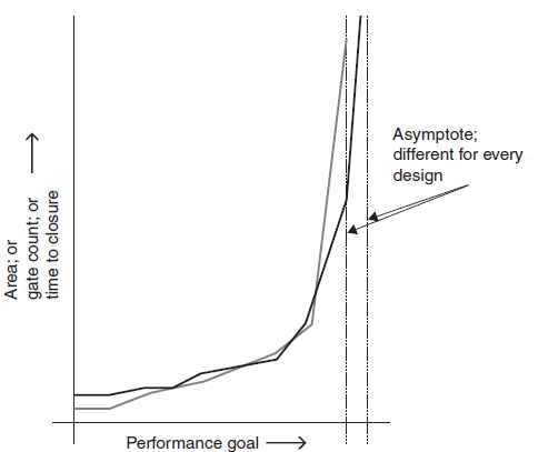
he resultant netlist would hit asymptotic performance limits as illustrated in Figure 2.1.
Typically, these asymptotes were within a percent or two of each other for a given block for the two versions of the library. It looked as if the pared-down library was just as effective as the larger full version, and the synthesis time was half or less for the pareddown version as opposed to the full version. It should be noted that as these asymptotes were approached, the “time to closure gap” tended to close, but this was faint praise for the full library if there was no real benefit until the very edge of the performance envelop was hit. I held my ground, but the design center was about to force me to give them what I knew to be an inferior stdcell library offering. Then we started the exercise of synthesizing a complex communication channel. It had both complex state machines and some significant arithmetic logic units in it, but these were not overly complicated as compared
with many modern designs. The full library synthesized the netlist across the performance targets chosen in anywhere from 25% to 40% the time that the pared-down library did. The full-library asymptote was about 15% higher than the pared-down version. In addition, the netlists for the full library were on average 85% the area, at the same performance, as the pared-down library results. We had met the RTL writer whose output needed the full-library offering.
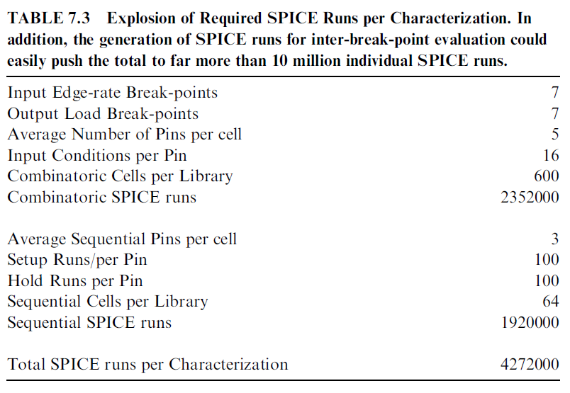
4.8 SPICE需要多少个run?
This is still considered viable from an engineering and economic point of view. However, in the case of digital design, the design industry has bought into the promise of the engineering design automation (EDA) industry over the past several decades. Specifically, EDA tools have allowed the level of transistors that can be effectively managed by a single design engineer to be greatly and continuously increased during that same period. In this case, spending days to weeks on simulation of a few dozen to a few hundred transistors (depending on the tasks’ level of complexity) is disastrous to a digital design cycle. Admittedly, the preceding analysis is for a digital IC device as opposed to a library development, but the mentality involved has translated itself to the digital library environment as well. When a new process, voltage, and temperature (PVT) corner characterization is requested by a design center, the next question is “When can I have it?” In addition, it is assumed that the delay in producing that characterization results from the limits of the computer resources required to produce the required simulations needed for the characterization as opposed to the engineering resources that could be needed to review and possibly rerun those simulations. The final analysis here is that the numbers in any given characterization file—whether timing arcs, power arcs, noise arcs, or capacitances—should be viewed cautiously by the user community.
So what kinds of issues can happen in an improperly tuned SPICE run? During a typical characterization effort, it could easily take more than 4 million or 5 million individual SPICE runs in order to make the measurements for perhaps a half dozen or
more input edge-rate break points by a half dozen or more output load break points. This is repeated for each of the dozen or more unique conditions for each of the several inputs per each of the several hundred stdcells in a typical design. These are further joined by the longer time frame required for setup-and-hold calculations are accomplished by treating the memory element (e.g., flop or latch) as a black box during simulations. These are required for each sequential element in the typical library (Table 7.3).
Typical issues that can easily arise in such a case are:
SPICE step-size mishandling;
inappropriate SPICE, absolute error tolerance (ABSTOL), relative error tolerance
(RELTOL), and charge tolerance (CRGTOL);
simulation ringing;
metastability; and
missed edges.
SPICE step size usually manifest itself in terms of incorrect output edge-rate measures because of SPICE converging at time steps that straddle the more appropriate points. Doing so causes the interpolation of the value being measured at points too far away from actuality, this then allows incorrect (or inaccurate) measure. Figure 7.2 gives a quick demonstration of this issue. Although SPICE itself can override the step size
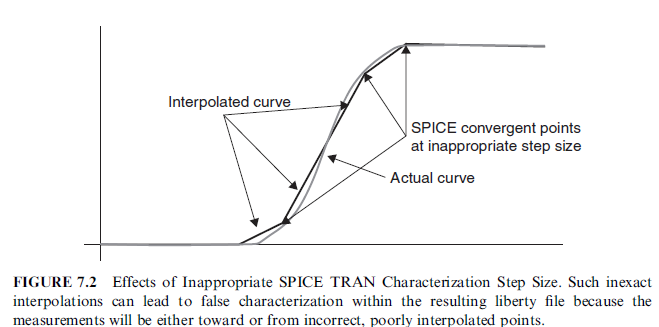
requested in a SPICE transient (TRAN) card, it is not foolproof and can therefore be difficult to diagnose. However, once diagnosed, it is easily remedied by just forcing tighter steps in the SPICE TRAN card. Note that there then is a penalty for step size: the tighter the step size, the longer the run time. In general, it is probably a good idea to define step size as equal to the desired level of accuracy in the timing section of the characterization file. If the desire is for accuracy to 10 pico-seconds, then make the step size no greater than this.
The next issue that can arise is incorrect RELTOL, ABSTOL, and CRGTOL. The way that SPICE works in TRAN analysis is that the tool takes the current state of the circuit simulation at every step in the requested time span of the run, together with the changes to the inputs for the next step, and tries to converge on the next state of the circuit. It does this by repeated approximation using one of several sequential approximate techniques. In general, a state approximation is generated, and then the relative change and the absolute change in the voltage and current state of each node from the previous approximation of that same step in the run is determined. If the change is too large compared to the relative tolerance and absolute tolerance numbers given by RELTOL and ABSTOL, or if the change in total charge tolerance is too large as compared
to CRGTOL, then the state of the circuit simulation is judged to be not yet converged and another successive approximate cycle is begun. This continues until such time that all nodes in the circuit do converge on voltage and current states that fulfill the
RELTOL and ABSTOL limits. For many combinational circuits, this is not an issue, but for sequential circuits, convergence can become an important and time-consuming hindrance. The usual solution is to increase the RELTOL and ABSTOL numbers in the
hopes of more quickly finding a convergence approximation. The issue with this is that the convergence approximation may be significantly off from the actual state that the circuit would be in under the same conditions.
Ringing will be discussed further in Chapters 9, 10, and 11, but suffice it here to say that it is demonstrable that any discontinuous change in a signal will cause a simulation of that change to oscillate over time. Although the oscillation should dampen out, it is still not real. There are real phenomena that produce the same thing in real circuits, but the two features are not correlated. Hence, any ringing in a SPICE simulation of a circuit that is not designed to cause such ringing is suspect. However, any measure of the various points of a characterization file will be around such signal discontinuities. Hence, every
measure may have ringing-induced inaccuracies. The bottom line here is that this means that the characterization file is nothing but a simulation of reality. It is not reality. This becomes a liberating realization. This means that the values in the various characterization files can be adjusted as desired for other reasons without giving up on accuracy because the original characterization file is only a representation as well. The modifications that this allows will be discussed shortly.
Metastability is the next reason for inaccuracies in a characterization file. As mentioned in the section on sequential stdcells, metastability is the possibility of a storage element going into an indeterminate state. It is a real event and can produce circuits that remain in such states for extended periods. Parasitic resistances and capacitances within any circuit, however, will eventually cause the given metastable sequential cell to resolve. The bad news is that the time taken can be vastly longer than the normal operating clock frequency of the logic in which such a sequential cell in used. What is even worse is that metastability is almost impossible to simulate. The closest that can usually be reached is that the output of a sequential cell tends to grow as a metastable point is approached. However, the actual metastable point is significantly small. Nonetheless, metastability is real. The only real way to solve this is to keep the setup and hold region sufficiently far away from the region where metastability is suspected. Methods of doing this are extensively discussed in Chapters 9, 10, and 11. One last reason that can cause inaccuracies in a characterization file are the actual missing or misinterpreted events within a SPICE result. Recall that a library characterization may involve 4 million or 5 million actual SPICE runs. Many times, two or three (or more) of these can be intelligently combined into multiple measurement runs. Doing such measurement run combination, however, can result in inappropriate measurements. Specifically, if a first or second measurement event in such a combined run does not occur as planned, for whatever reason, then subsequent measurements that occur in the same run should be questioned. A missed event, usually an edge on an output signal, could easily be interpreted as an edge event for an earlier missed event. As a result,
several measures would be incorrect. These measures would be spread throughout any resulting characterization file. The one possible means to determine such failure, perhaps the only means, is to intensely inspect a resulting characterization file. Comparison of the results for a given pin on a given cell to similar pins in similar cells should be reviewed for consistency. Similar comparisons across the input edge rate or output load measures for a given pin can be reviewed for significant changes. Comparisons of similar pins within a cell should be reviewed. Finally, comparison across similar PVT characterization
files also should be done.
Note that this process is not automatable. When a failure mechanism is identified, diagnostic tests can be automated and run on any resulting characterization file that is built from that point onward, but each new characterization file needs to be reviewed for previously unseen (or at least previously undetected but present) failure mechanism. This will be discussed further in Chapter 13.
Earlier in the section I mentioned that any characterization file, by the very fact that it is based on simulations that cannot be completely accurate, is nothing more than a representation of reality. This representation is designed to be useful to the chip-level synthesis and chip-level timing and power closure tools. Knowing this is the case, it should be easy to convince a design-center engineer that further modifications to a resulting characterization file, in order to allow for more efficient synthesis (as an example), will do nothing but allow for better or more efficient design-level synthesis. Chapters 9, 10, and 11 discuss ways to force monotonic behavior on a characterization file. There is a further discussion on ensuring that all measurement values are positive (or at least nonnegative), with the possible counter reasoning of the need for useful skew design techniques. The preceding argument suggests that these methods are valid.
4.9 【IC模拟版图设计】与非门版图设计视频教程
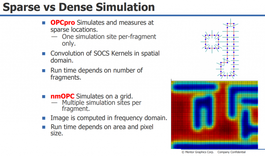
5.光学临近校正
Mentor的OPC软件是Calibre nmOPC,Synopsys的OPC软件是Proteus
新闻上说英特尔14nm的工艺产品都出来了,想知道论坛里面有多少人做过32nm,28nm,22nm,20nm工艺,
它们与其他工艺有什么不一样的地方?
答:
| 做过12nm,印象深刻有以下几点: (1)所有poly都要求竖着(28nm只有低压mos gate要求竖着),这样像PAD layout,因为横竖方向都要放,就要做两个版本的layout. (2)因为M1 space太小,会分两次做,所以M1有两层mask,一个loop内的m1个数不能是基数。不然不好分Mask。 (2)power gnd metal不能成环,所以guardring m1要断开,power gnd不能做成网络,一般做成树枝状。 (3)PR区域会有很多奇怪的drc,很难解决。记得有个drc是M2宽度在某个范围内时,space只能在一定范围内,而不是以前的space要求至少多少。 (4)密度要求很严格,所以一般一个模块把器件调进来,先跑drc,确保poly AA密度不超再连线。 (5)lvs都容易过,drc多了很多,麻烦很多。 (6)gate加两条dummy poly (7)stdcell边上要加边界cell,但是stdcell中间不能出现边界cell |
答上:
| 1 poly 同一个方向是因为fin 都是同一个方向,fin一般水平, poly必须垂直放。28是平面工艺 2 M1 应该采用的是LELE的double patterning 方式,要求相邻的track 不在同一张mask,pitch 估计是48 所以是按照track拆分,这样需要保证和外面的pattern 如果基数有可能和外面pattern是同一个mask造成OPC拆分不出来。如果是14nm 的话应该没有这个rule 因为是64 的pitch 是按照相邻pattern 来拆分,拆分方式不同。 3 不能成环?是单层metal不能成环吧?跳线还是可以的。单层metal不能成环是因为在不同方向的min width 不一样,如果都足够大也是可以的。 如果都比较小的时候,OPC litho 不能保证二维图形的target 4 space 在一定范围也是OPC litho的要求。在某些特定的pitch会特别难做,一般forbidden zone 是min pitch 的3~5 倍的区间。 5 density要求不仅来自于CMP 还来自于etch 的process,特别对fin density 和Poly density都很敏感 6 多加poly dummy 是因为fin cut 的原因在fin 边缘会变成一个斜坡,同是V0 是通过外延方式生长在fin上,多加poly 是应力的原因 你还没有做到8nm,metal还要加cut layer,DRC会再加一个数量级。 |
对 SRAM 的一些偏见
正文:
刚入行的时候SRAM用得很多。 通信芯片,需要存储很多数据。
几年后换到一家百年老店,惊讶地发现绝大部分PDK里没有memory compiler。 Analog工艺PDK全都没有memory compiler,需要定制。 想了想,觉得老店很有道理。 开店是为了赚钱,是不择手段的。 弃用,或慎用SRAM, 也是老店八卦六十四式的一招。
SRAM对yield是有影响的,特别是SRAM大的时候。 坏一个bit, 片子就废了。 为了提高yield, SRAM要多做两个column,作为备用,需要的时候用备用代替主体里坏掉的column。具体细节做起来还是有些麻烦的。 即使有备用,有的时候yield还是低一些。
SRAM对DFT是有影响的。 通常SRAM需要mbist。 mbist不是免费的,是实实在在的门,大致1k~2k。 mbist如何启动,如何读出,都是有些麻烦的。 如果SRAM本身才几百位,就得不偿失了。
SRAM如果是Foundary的IP,是要银子的。 如果准备打价格战,拼价格的,每个片子IP的费用就要考量了。
当然,SRAM有很多优点。 功耗肯定是比同样位数的 DFF 矩阵要低。 这时你那贼特嘻嘻的主管就会问你,能不能把 DFF 矩阵功耗降到和 SRAM 一样低。 很多时候,好的工程师会把貌似不可能的事情变成可能。 这个就是工程设计的魅力了。
有些设计中SRAM是完全必要的,如大部分MCU。
抛砖引玉吧。 欢迎道友批评讨论。
答:CELL是不可能的,所谓自己定制,是因为mem compiler对一定范围大小的周边电路是完全一致的,并不是最优解,这个时候要想最快速度,就需要自己去定制。
但这种定制还是基于FOUNDARY提供的CELL和模型。主要还是优化周边电路,并不是定制CELL。
老的工艺的时候,还有一个专门做SRAM的公司会自己做些CELL。先进工艺,需要格外的OPC修正,设计公司是不可能拿到工厂的光刻机和光阻参数的,只能使用工厂提供的CELL。
SMIC工艺tapeout前要加OPC block layer,请问这个是什么层?干什么用的?
| opc是光学近似修正, 一般180nm以下会对光刻图案做修正,使光刻机得到最大的曝光window,目的是使曝光刻蚀后的图案尽量与你layout设计中的一致。 opc block layer应该就是这个区域不需要做opc,比如ram/rom,从foundry拿来的bit-cell已经做过opc. ESD器件比较大,可以不用做OPC的 |
Calibre PTO flow
Calibre is the Market Leader for Entire Post Tape Out Flow
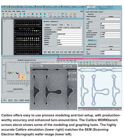
Calibre DRC, LVS and DFM overview