2018-08-12
一、作用:RTL ——- > 优化过的netlist(logic Circuit)。
二、synthesis flow:
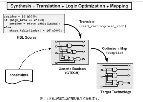
三、synthesis = translation + logic optimization + gate mapping
- Translation:将RTL代码转化成GTECH库元件组成的逻辑电路。
- gate mapping:将GTECH库元件组成的逻辑图转换到目标工艺库上,形成.dcc文件。
- logic optimization:根据所需时延、功耗、面积等约束条件进行优化。
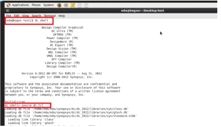
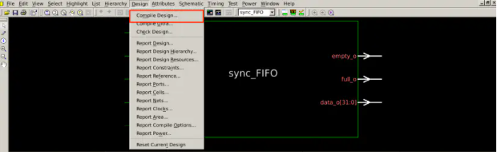
四、lab流程–两种工作模式:脚本和图形化界面
一、脚本内容设置:dc.tcl
1.设置库链接:
 set search_path  {/home/eda/eda/synopsys/dc/dc_2012/libraries/syn}
 set target_library {class.db}     //供应商提供目标库
 set link_library  {* class.db}    //指定压焊块工艺库名称和所有其他的宏单元,RAM、ROM等
 set symbol_library {class.sdb}    //包含工艺库中的单元图形表示的库名称
2.读入.v文件
read_file -format verilog {/home/eda/Desktop/test/sync_FIFO.v}
3.设置约束条件
 set_max_area 0  //让综合后的面积越小越好
 set_max_fanout 4 sync_FIFO   // 约束cell的最大扇出,扇出过大会使cell delay变慢
 set_max_transition 0.5 sync_FIFO
 compile -exact_map //综合优化
4.保存db和netlist:
 sdc /home/eda/Desktop/test/sync_FIFO.sdc  //保存.db文件
 write -format verilog -hierarchy -output /home/eda/Desktop/test/netlist.v
 write_sdc /home/eda/Desktop/test/sync_FIFO.sdc //保存时序约束文件(.sdc文件)
 write_sdf /home/eda/Desktop/test/sync_FIFO.sdf  //保存标准延时文件(.sdf文件)
5.report PPA:
 report_area > /home/eda/Desktop/test/area.area_rpt
 report_constraint -all_violators > /home/eda/Desktop/test/cons.constraint_rpt
 report_timing > /home/eda/Desktop/test/timing.timing_rpt
6.运行脚本:
  dc_shell  //启动DC
  source dc.tcl  //运行脚本
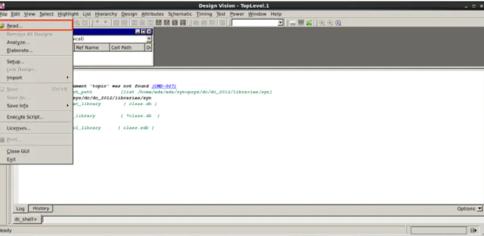
二、图形化界面操作:
1.进入gui界面
dc_shell -gui //图形化界面打开窗口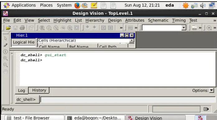
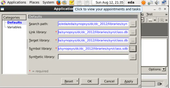
2.设置库–打开File菜单栏下的Setup进行设置
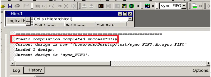
3.读RTL文件
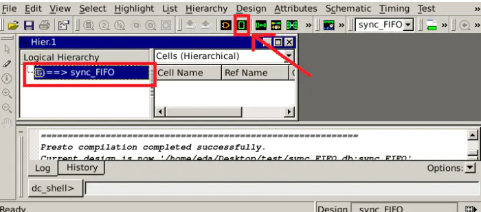
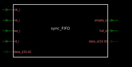
4.加载符号图形
5.设置约束条件 –此处可命令操作也可图形操作
 create_clock -name "clock" -period 20 -waveform { 010 } { clk_i } //时钟约束条件
set_dont_touch_network { rst_i }  //复位
 set_input_delay 12 -clock clock {we_i rd_i data_i}  //we_i, rd_i, data_i
 set_output_delay 12 -clock clock { empty_o full_o data_o}  //full_o等
 set_max_area 0
 set_max_fanout 4 sync_FIFO
 set_max_transition 0.5 sync_FIFO
6.优化综合
7.查看报告
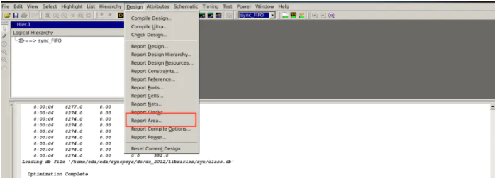
五、report分析
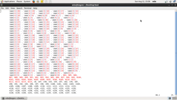
- vi编辑器进入生成的netlist
- 最后进行时序分析+面积报告分析
end
作者:打着石膏脚的火星人
链接:https://www.jianshu.com/p/858079948adb/
来源:简书
简书著作权归作者所有,任何形式的转载都请联系作者获得授权并注明出处。