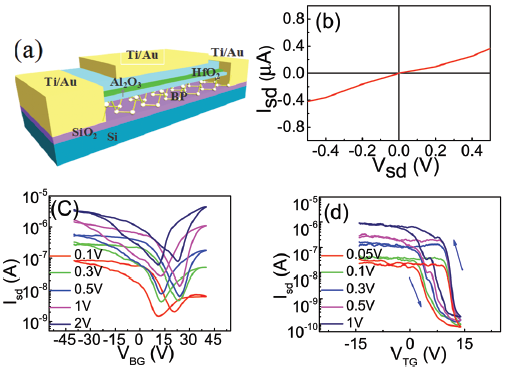
The electron affinity of BP is about 4.4 eV and the band gap of the bulk and monolayer BP is 0.3 eV and about 2.0 eV, respectively[1].
GeSe process a small work function (WF) of 4.4–4.8 approaching to the electron affinity of to the electron affinity of InSe (4.6 eV)[2].
Bulk GeSe has an electron affinity of about 4.09 eV and has an energy bandgap of 1.1–1.2 eV[3]
The results indicate that the few-layer GeSe presents a robust direct band gap, which decreases with increasing the thickness from bilayer (1.15 eV) to six-layer (1.00 eV) around the X point. Furthermore, the work function increases rapidly from monolayer (4.44 eV) to trilayer (4.95 eV).[4]
The work functions of as-prepared 1- to 6-layer MoS2 nanoflakes were 5.15 − 5.39 eV and increased with increasing layer number[5].
Our findings reveal that the semiconductor 2H-MoS2 exhibits both n- and p-type behavior, and the work function as measured by the Kelvin probe is found to vary from 4.4 to 5.3 eV.[6]
We show that the Schottky barriers between metals and the MoS 2 cannot be predicted by simply comparing the metal work function to the MoS 2 electron affinity[7]
参考文献
[1] Charge trap memory based on few-layer black phosphorus
[2] Reversible Half Wave Rectifier Based on 2D InSe/GeSe Heterostructure with Near-Broken Band Alignment
[3] WSe2/GeSe heterojunction photodiode with giant gate tunability
[4] Layer-controlled band alignment, work function and optical properties of few-layer GeSe
[5] Layer-number-dependent Work Function of MoS2 Nanoflakes
[6] Impurities and Electronic Property Variations of Natural MoS2 Crystal Surfaces
[7] Defect-Dominated Doping and Contact Resistance in MoS2